OrCAD Capture Constraint Manager PCB Flow
By Jarret
General Notes
Section titled “General Notes”-
Here is the link to the course.
-
Follow the same steps as above for starting this project; however, DO NOT download the lab database into OneDrive (or any form of online storage), as this caused problems down the line for me archiving the project, etc.
-
When the lab PDF tells you to save the project, and an error comes up when you do this, first check if the lab PDF says anything about errors coming up. If it does, you are good to move on. If it does not, click on the error to see if you can fix it before moving on.
Requirements
Section titled “Requirements”-
Access to Capture CIS 17.4
-
Access to PCB Editor 17.4
-
Also helpful to have finished the courses before this one on the learning map.
Resources
Section titled “Resources”- Website to learn about package types as they are once again mentioned in this lab
Introduction
Section titled “Introduction”This course covers bringing a design over from the OrCAD Capture schematic editor to the PCB Editor. This will cover many aspects of the design process and in particular the use of the constraint manager to set parameters for the PCB layout. Please note that at the moment Cadence only offers the 17.4 version of this course, but you can follow along using the 22.1 Capture software just fine. However you will need access to both the 22.1 and 17.4 PCB Editor if you choose to use the 22.1 Capture software. This guide will cover some of the differences between the 22.1 and 17.4 software as they show up in the course. (Recommended to just use the 17.4 software)
Module 1 and Database Downloads
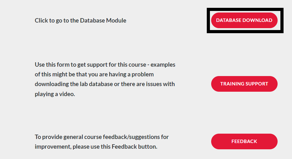
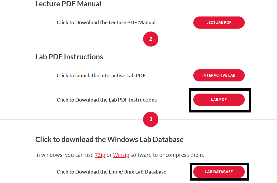
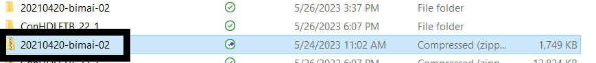
Section titled “Module 1 and Database Downloads”Module 1 of the course simply contains an overview of what the course will cover. It is still important to read over this and gather an understanding of what you will be learning. Before starting the course you should head to the Database Downloads module of the course. On the Module 1 page, click “Database Downloads” and save the folder “Lab Database” to a location on your computer. I recommend making this folder easy to access as you will be navigating to it a lot throughout the course. Right-click on this folder, and click “Extract all”. Also, open up the “Lab PDF” in a new tab. See below.
Module 2
Section titled “Module 2”The second module covers some basics of operating the constraint manager such as adding properties and creating classes. The first lab will involve modifying or adding some environment variables. The easiest way to do this in my opinion is to simply launch the environment variable page by entering Environment Variables into the windows search bar, then selecting the “Edit the system environment variables” option. This will open a new system properties window, where at the bottom you will see a button which says Environment Variables… (Forewarning, the pictues given by the lab book are a bit outdated so the buttons are not going to be where shown, but they will still all be in the same windows somewhere, you just have to find them.) Click the button to edit your environment variables. From here add your CDS_SITE and HOME variables but be sure to save any existing environment variables of the same name by changing the name beforehand.
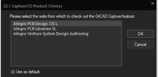
When the lab book tells you to choose the product “OrCAD PCB Designer Professional,” actually choose the “Allegro PCD Design CIS L,” as we do not have their option available. After this, the lab will walk you through using the constraint manager. Some small details to note: first when the lab has you using the differential pair automatic setup tool, on the 22.1 software if you simply enter _P and _N into the +Filter and -Filter fields, pressing Enter will automatically create the differential pair, instead of populating the fields as the lab has you do. Finally when the lab has you creating net classes, there is a step involving creating a class with the BNC2, BNC3, OUTA, and OUTB nets. If you are using the 22.1 software, do not worry about looking for the OUTA and OUTB nets as they are included in the BNC2 and BNC3 nets, thus you only need to include the two BNC nets in the net class.
Module 3
Section titled “Module 3”Module 3 involves the transition from design entry in Capture CIS to circuit board layout using the PCB Editor. If using the 22.1 Capture CIS software, you will find the *.brd file in the project manager within the layout folder. To launch the PCB Editor you can either double click on the *.brd file or you can right click the file then select Launch PCB Editor. When the PCB Editor asks you to choose a product, choose “Allegro PCB Venture”, instead of “Allegro PCB Designer”, as we do not have access to that option. In lab 3-4 for this section you will be asked to use the automatic router in the PCB Editor. If you have already done the Allegro Design Entry HDL Front-to-Back Flow course then you should be familiar with the issue that arises from this. Since we do not yet have access to the 22.1 routing license, you must use the 17.4 software to run the auto router. For instructions on how to install the 17.4 software, refer to the getting started section of this website. Once this software has been installed, you can simply open the *.brd file you were working on in the 17.4 software, follow the lab instructions on running the auto router, then save the changes made to the file and reopen it in the 22.1 software. One of the biggest differences between the 22.1 and 17.4 software that shows up in the lab is the design synchronization tool. In the 22.1 software there is no one “Design Sync” button as there is in the 17.4 edition. Instead there are two options. If you have made changes in the schematic editor, then choose Update Layout to sync the PCB design. If you have made changes in the PCB Editor then choose the Update Schematic to sync the schematic design. Aside from this the update layout and update schematic windows should look very similar to the design sync window from the 17.4 software and should be easy to follow along with.
In the beginning of this lab, you have to navigate using the browse button to where the Cadence software is downloaded on your computer. Normally, they are in the “This PC”>“OS (C)”>“Cadence”>“SPB_17.4” directory. If not, search a cadence app in the search window on the bottom left of your computer, left click on the selection and choose “Open File Location,” and you should be able to see where the data is downloaded.
Module 4: Engineering Changes
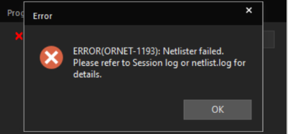
Section titled “Module 4: Engineering Changes”The final module covers some more basics of design synchronization such as synchronizing changes to the constraint manager and regenerating a netlist. These labs will involve using the design sync tool as well as the auto router, so be sure to read the module 3 guide to understand how to deal with the issues arising from these tools. One other issue you may encounter in this lab is netlisting errors. If the netlist fails to generate then you will see the error message shown below (to the left). If this happens then open the session log window by choosing View > Session Log Window from the pull down menu. The session log will print out the errors the netlist generator is encountering, an example of which can be seen below (to the right). In this case there was a duplicate reference designation in the resistor ‘R6’, which could be fixed by editing the resistor properties and changing the resistor’s name.